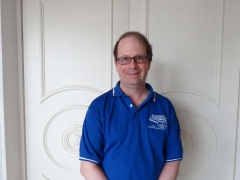
Speaker: Professor Raynald Gauvin, McGill University
Time: 16:30-17:30, Jly. 24 (Friday)
Location:Room 215, School of Materials Science and Engineering (MSE)
Abstract: The new generation of Field Emission Scanning Electron Microscope (FE-SEM) can perform high resolution imaging at incident electron beam energy below 1 keV. Images with resolution smaller than 2 nm are now guaranties by various manufacturers. Since imaging below 1 keV allows obtaining surface details of nanomaterials and reduces beam damage for sensitive materials, it is clear that electron microscopy is now entering in a new era. With FE-SEMs that can operate in the 50 eV to 30 keV mode with many images modes like conventional bulk secondary electron (SE) or backscattered electron (BSE) imaging or new scanning transmission electron microscopy (STEM) imaging of transparent materials in bright field or dark field mode, the versatility of these microscopes is obvious. Also, if we keep in mind that we can also perform quantitative x-ray microanalysis with state of the art SDD EDS detectors and crystallographic characterization of materials with EBSD detectors, FE-SEM has a very bright future. Its importance in science and technology will growth faster than ever because we have now microscopes that can deliver enough current with high spatial resolution to fully exploit the advantages of low voltage scanning electron microscopy as predicted by Von Ardenne as far as 1942. This paper will present new results for the characterization of various nanomaterials obtained with the Hitachi SU - 8000 cold field FE-SEM. This FE-SEM has 1 SE lower detector, 2 SE upper detectors with various modes of energy filtration, a five quadrant BSE detector, a STEM detector that works in bright field, an electron convertor that allows to use the SE lower detector for dark field STEM imaging, a 80 mm2 SDD EDs detector (Oxford Instrument) and the EBSD Nordlys II System (Oxford Instrument). Also, high resolution results with the new Hitachi SU – 8230 with the new Auto Flash technology equipped with the 1.2 Sr SDD EDS Bruker FlatQuad detector will be presented.
Biography: Pr. Raynald Gauvin received his Ph.D. in 1990 at École Polytechnique de Montréal in Metallurgical Engineering. He was then appointed as an assistant professor in Mechanical Engineering at Sherbrooke University where he became associate Professor in 1995 and full Professor in 1998. In 2001, he joined the department of Mining and Materials Engineering of McGill University, Montréal, Canada, as a full Professor. Pr. Gauvin’s research interest are related in developing new methods to characterize the microstructure of materials using high resolution scanning electron microscopy with x-ray microanalysis and Monte Carlo simulations. He has more than 200 papers in scientific journals and conference proceedings. He was Invited Speaker in more than 80 international scientific conferences. He won several scientific prices, most notably the 31st Canadian Materials Physics Medal in 2007 by the Metallurgical Society of the Canadian Institute of Mining, the Heinrich Award in 1997 from the Microbeam Analysis Society of America and the Prix d'excellence du président de l’École for the best Doctorate Thesis defended in 1990 at École Polytechnique de Montréal. Pr. Gauvin is currently the President of the Inter American Societies of Electron Microscopy (CIASEM). He was President of the Microbeam Analysis Society of America (MAS) from 2005 to 2006, President of the Microscopical Society of Canada (SMC) from 2001 to 2003 and President of the International Union of the Microbeam Analysis Societies (IUMAS) from 2000 to 2005.

